| CPC G09G 3/20 (2013.01) [G11C 19/287 (2013.01); G09G 2300/0426 (2013.01); G09G 2310/0286 (2013.01); G09G 2310/061 (2013.01); G09G 2310/08 (2013.01)] | 20 Claims |
|
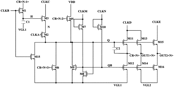
1. A shift register unit, comprising a first input circuit, an output control circuit, an output circuit, a fourth node control circuit, and a second noise reduction circuit;
wherein the first input circuit is connected to a first node, and is configured to output a first input signal to the first node in response to a first control signal, wherein the first input signal is a constant high level signal;
the output control circuit is connected to the first node and a second node, and is configured to output an output control signal to the second node;
the output circuit comprises an output terminal, and the output circuit is connected to the second node, and is configured to output an output signal to the output terminal under control of a level of the second node;
the fourth node control circuit is connected to the second node and a fourth node, and is configured to control a level of the fourth node under control of the level of the second node; and
the second noise reduction circuit is connected to the second node, the fourth node, and the output terminal, and is configured to perform noise reduction on the second node and the output terminal under control of the level of the fourth node;
wherein the output terminal comprises a shift output terminal and at least one scan signal output terminal;
wherein the at least one scan signal output terminal comprises a first scan signal output terminal and a second scan signal output terminal, and the second noise reduction circuit comprises an eleventh transistor, a twelfth transistor, a thirteenth transistor, and a fourteenth transistor;
a gate electrode of the eleventh transistor is connected to the fourth node, a first electrode of the eleventh transistor is connected to the second node, and a second electrode of the eleventh transistor is connected to a second voltage terminal to receive a second voltage;
a gate electrode of the twelfth transistor is connected to the fourth node, a first electrode of the twelfth transistor is connected to the shift output terminal, and a second electrode of the twelfth transistor is connected to the second voltage terminal to receive the second voltage;
a gate electrode of the thirteenth transistor is connected to the fourth node, a first electrode of the thirteenth transistor is connected to the first scan signal output terminal, and a second electrode of the thirteenth transistor is connected to a third voltage terminal to receive a third voltage; and
a gate electrode of the fourteenth transistor is connected to the fourth node, a first electrode of the fourteenth transistor is connected to the second scan signal output terminal, and a second electrode of the fourteenth transistor is connected to the third voltage terminal to receive the third voltage,
wherein the output circuit comprises a fifteenth transistor, a sixteenth transistor, a seventeenth transistor, and a second capacitor;
a gate electrode of the fifteenth transistor is connected to the second node, a first electrode of the fifteenth transistor is connected to a fourth clock signal terminal to receive a fourth clock signal as the output signal, and a second electrode of the fifteenth transistor is connected to the shift output terminal;
a gate electrode of the sixteenth transistor is connected to the second node, and a first electrode of the sixteenth transistor is connected to the fourth clock signal terminal to receive the fourth clock signal as the output signal, and a second electrode of the sixteenth transistor is connected to the first scan signal output terminal;
a gate electrode of the seventeenth transistor is connected to the second node, and a first electrode of the seventeenth transistor is connected to a fifth clock signal terminal to receive a fifth clock signal as the output signal, and a second electrode of the seventeenth transistor is connected to the second scan signal output terminal; and
a first terminal of the second capacitor is connected to the second node, and a second terminal of the second capacitor is connected to the shift output terminal,
wherein the shift register unit further comprises a second input circuit;
the second input circuit is connected to the first node, and is configured to input a second input signal according to a second control signal;
the second input circuit comprises a charging sub-circuit, a storage sub-circuit, and an isolation sub-circuit;
the charging sub-circuit is connected to a blanking node, and is configured to input the second control signal to the blanking node in response to a sixth clock signal;
the storage sub-circuit is connected to the blanking node, and is configured to store a level of the second control signal input by the charging sub-circuit; and
the isolation sub-circuit is connected to the blanking node and the first node, and is configured to input the second input signal under control of a level of the blanking node and a seventh clock signal;
the charging sub-circuit comprises an eighteenth transistor, a gate electrode of the eighteenth transistor is connected to a sixth clock signal terminal to receive the sixth clock signal, a first electrode of the eighteenth transistor is connected to a blanking control terminal to receive the second control signal, and a second electrode of the eighteenth transistor is connected to the blanking node;
the storage sub-circuit comprises a third capacitor, a first terminal of the third capacitor is connected to the blanking node, and is configured to store a level of the second control signal; and
the isolation sub-circuit comprises a nineteenth transistor and a twentieth transistor, and a gate electrode of the twentieth transistor is connected to a seventh clock signal terminal to receive the seventh clock signal, a first electrode of the twentieth transistor is connected to a second electrode of the nineteenth transistor, and a second electrode of the twentieth transistor is connected to the first node.
|