| CPC G09G 3/20 (2013.01) [G11C 19/28 (2013.01); G09G 2310/0267 (2013.01); G09G 2310/0286 (2013.01)] | 11 Claims |
|
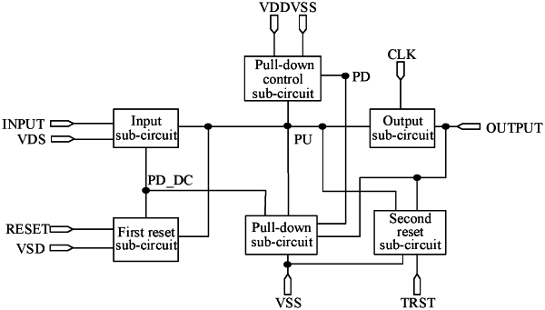
1. A shift register, comprising:
an input sub-circuit, a first reset sub-circuit, an output sub-circuit, a pull-down sub-circuit, a pull-down control sub-circuit and a second reset sub-circuit, wherein
the input sub-circuit is configured to, under control of a signal input terminal, provide a signal of a first voltage source to a pull-up node and a first node respectively;
the first reset sub-circuit is configured to, under control of a reset terminal, provide a signal of a second voltage source to the pull-up node and the first node respectively;
the output sub-circuit is configured to, according to a level of the pull-up node, output a signal of a clock signal terminal to a signal output terminal;
the pull-down control sub-circuit is configured to, according to the level of the pull-up node and a signal of a third voltage source, control a level of a pull-down node;
the pull-down sub-circuit is configured to, according to a level of the first node, output a level of a fourth voltage source to the pull-down node, and, according to the level of the pull-down node, output the level of the fourth voltage source to the pull-up node and the signal output terminal; and
the second reset sub-circuit is configured to, under control of a total reset terminal, reset the pull-up node and the signal output terminal.
|