| CPC G09G 3/006 (2013.01) [G02F 1/13452 (2013.01); G09G 3/20 (2013.01); H01L 23/3114 (2013.01); H01L 23/4824 (2013.01); H01L 23/4985 (2013.01); H05K 1/0268 (2013.01); G09G 2300/0413 (2013.01); G09G 2300/0426 (2013.01); G09G 2330/12 (2013.01); H05K 1/028 (2013.01); H05K 1/189 (2013.01); H05K 2201/10128 (2013.01)] | 17 Claims |
|
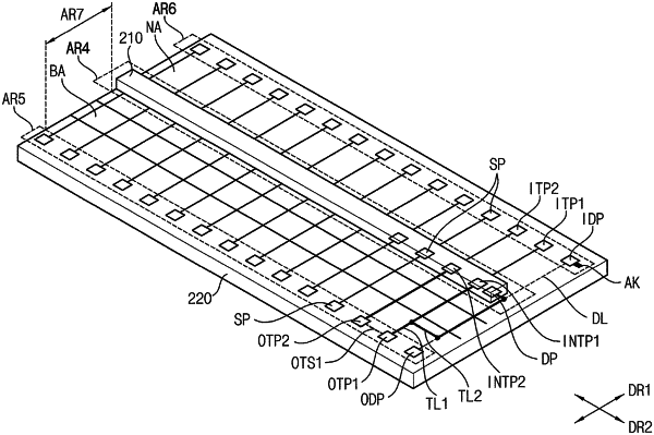
1. A chip-on-film package comprising:
a base substrate on which a first pad region extends on a first side defining one side of the base substrate, a second pad region extending on a second side defining an opposite side of the base substrate to the one side of the base substrate, a third pad region located between the first pad region and the second pad region, a first region located between the first pad region and the third pad region, and a second region located between the third pad region and the second pad region are defined;
a plurality of first-pads and a first dummy-pad disposed on the first pad region;
a plurality of second-pads and a second dummy-pad disposed on the second pad region;
a plurality of third-pads and a third dummy-pad disposed on the third pad region;
a first detection line disposed on the base substrate, wherein the first detection line includes a first sub-detection line connected between a first first-pad of the first-pads and a first third-pad of the third-pads and a second sub-detection line connected between a second first-pad of the first-pads and a second third-pad of the third-pads, the first sub-detection line being connected to the second sub-detection line in the first pad region to form a first loop between the first third-pad and the second third-pad; and
a second detection line disposed on the base substrate, wherein the second detection line is connected between the third dummy-pad and the first detection line, the second detection line being connected to the first sub-detection line in the first region to form a second loop between the third dummy-pad and the first third-pad.
|