US 11,748,541 B2
Methods for engineering integrated circuit design and development
Bertrand Irissou, San Jose, CA (US); John M. Hughes, Hartford, CT (US); Lucio Lanza, Palo Alto, CA (US); Mohamed K. Kassem, Carlsbad, CA (US); Michael S. Wishart, Hillsborough, CA (US); Rajeev Srivastava, Austin, TX (US); Risto Bell, San Jose, CA (US); Robert Timothy Edwards, Poolesville, MD (US); Sherif Eid, Sunnyvale, CA (US); and Greg P. Shaurette, Tahoe City, CA (US)
Assigned to efabless corporation, San Jose, CA (US)
Filed by efabless corporation, San Jose, CA (US)
Filed on Oct. 25, 2021, as Appl. No. 17/510,315.
Application 17/510,315 is a continuation of application No. 16/583,170, filed on Sep. 25, 2019, granted, now 11,182,526.
Application 16/583,170 is a continuation of application No. 15/633,186, filed on Jun. 26, 2017, granted, now 10,452,802, issued on Oct. 22, 2019.
Claims priority of provisional application 62/359,858, filed on Jul. 8, 2016.
Prior Publication US 2022/0043956 A1, Feb. 10, 2022
Int. Cl. G06F 30/39 (2020.01); G06F 30/30 (2020.01); G06F 30/33 (2020.01); G06F 30/367 (2020.01); G06F 30/392 (2020.01); G06F 30/398 (2020.01); G06F 30/3323 (2020.01); H01L 23/00 (2006.01); G06F 119/18 (2020.01)
CPC G06F 30/39 (2020.01) [G06F 30/30 (2020.01); G06F 30/33 (2020.01); G06F 30/3323 (2020.01); G06F 30/367 (2020.01); G06F 30/392 (2020.01); G06F 30/398 (2020.01); H01L 23/573 (2013.01); G06F 2119/18 (2020.01)] 20 Claims
OG exemplary drawing
 
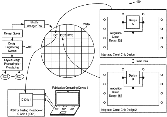
1. A method for accommodating a plurality of designs on a shuttle, comprising:
receiving a first design of a first system-on-chip (SoC) from a first user account with a request to fabricate the first SoC;
receiving a second design of a second SoC with a request to fabricate the second SoC;
determining that the first and second designs are to be fabricated on a semiconductor wafer;
providing the first and second designs to a shuttle manager tool to reserve spots of the first and second designs on the semiconductor wafer; and
sending a request to a fabrication entity to fabricate the first and second designs on the semiconductor wafer.