US 11,748,252 B2
Data write from pre-programmed register
Thomas J. Sheffler, San Francisco, CA (US); Lawrence Lai, San Jose, CA (US); Liang Peng, San Jose, CA (US); and Bohuslav Rychlik, San Diego, CA (US)
Assigned to Rambus Inc., San Jose, CA (US)
Filed by Rambus Inc., San Jose, CA (US)
Filed on Dec. 2, 2021, as Appl. No. 17/540,437.
Application 17/540,437 is a continuation of application No. 16/735,303, filed on Jan. 6, 2020, granted, now 11,204,863.
Application 16/735,303 is a continuation of application No. 15/882,847, filed on Jan. 29, 2018, granted, now 10,552,310, issued on Feb. 4, 2020.
Application 15/882,847 is a continuation of application No. 15/497,126, filed on Apr. 25, 2017, granted, now 9,898,400, issued on Feb. 20, 2018.
Application 15/497,126 is a continuation of application No. 14/637,369, filed on Mar. 3, 2015, granted, now 9,658,953, issued on May 23, 2017.
Application 14/637,369 is a continuation of application No. 13/383,205, abandoned, previously published as PCT/US2010/039095, filed on Jun. 17, 2010.
Claims priority of provisional application 61/235,564, filed on Aug. 20, 2009.
Prior Publication US 2022/0206936 A1, Jun. 30, 2022
This patent is subject to a terminal disclaimer.
Int. Cl. G06F 12/02 (2006.01); G11C 7/22 (2006.01); G11C 8/10 (2006.01); G11C 7/10 (2006.01)
CPC G06F 12/023 (2013.01) [G11C 7/1006 (2013.01); G11C 7/1039 (2013.01); G11C 7/22 (2013.01); G11C 8/10 (2013.01); H05K 999/99 (2013.01); G06F 2212/2024 (2013.01); G11C 2207/107 (2013.01)] 20 Claims
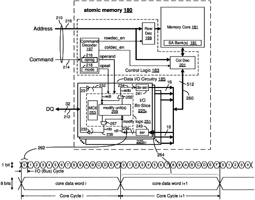
OG exemplary drawing
 
1. A memory controller component to control a memory integrated-circuit (IC) having a programmable register and a memory core, the memory controller component comprising:
a command/address interface;
a data interface; and
control circuitry to:
output, to the memory IC, a data-write command via the command/address interface and write data via the data interface, the data-write command instructing the memory IC to write the write data to the memory core;
output, via the command/address interface, a register-write instruction and corresponding data values to the memory IC, the register-write instruction instructing the memory IC to store the data values within the programmable register; and
output a memory access command and an address value to the memory IC via the command/address interface, the memory access command instructing the memory IC to write the data values, sourced from the programmable register, to the memory core at locations indicated by the address value.