| CPC G06F 9/3832 (2013.01) | 20 Claims |
|
1. An apparatus comprising:
a graphics processor comprising computation circuitry to:
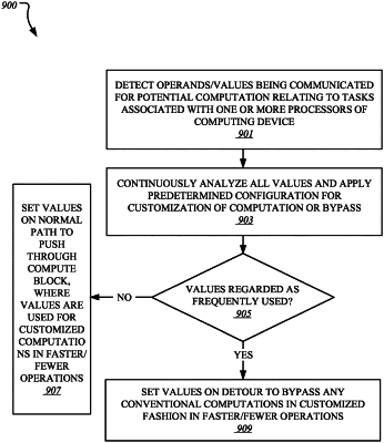
implement a frequently-used data value (FDV) configuration that is to identify a plurality of FDVs, wherein the FDV configuration is to provide a data list consisting of a set of data values defined as FDVs;
apply the FDV configuration to input data received at the computation circuitry, the input data to be used in computational tasks executed by the computation circuitry;
identify, based on the FDV configuration, occurrence in the input data of defined FDVs from the set of data values and of one or more non-FDVs, wherein the one or more non-FDVs consist of other data values that are not comprised in the set of data values;
for the identified FDVs of the input data, cause the identified FDVs to bypass the computational tasks; and
for the one or more non-FDVs of the input data, cause the one or more non-FDVs to be processed by a finite state machine (FSM) implemented by the computation circuitry, wherein the FSM is to:
provide a common primitive for convolution and full connection computation for the computational tasks;
combine memory read accesses; and
merge two or more mathematical operations of the computational tasks.
|