| CPC G06F 3/0446 (2019.05) [G06F 3/0412 (2013.01); G06F 3/0443 (2019.05); H10K 59/40 (2023.02); G06F 2203/04103 (2013.01); G06F 2203/04111 (2013.01); G09G 3/3233 (2013.01); G09G 2300/0426 (2013.01); G09G 2300/0809 (2013.01); G09G 2320/0238 (2013.01); H10K 59/122 (2023.02)] | 17 Claims |
|
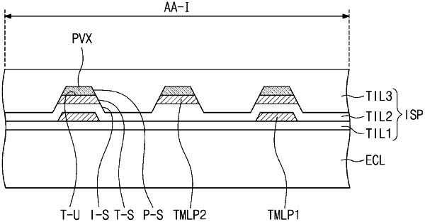
1. A display device comprising:
a display panel comprising a base layer, a circuit element layer comprising a transistor disposed on the base layer, a display element layer comprising a light emitting element connected to the transistor, and a thin film encapsulation layer covering the display element layer; and
an input sensing panel comprising a first sensing insulating layer disposed directly on the thin film encapsulation layer, a first conductive layer disposed on the first sensing insulating layer, a second sensing insulating layer covering the first conductive layer, a second conductive layer disposed on the second sensing insulating layer, a passivation layer disposed on the second conductive layer, and a third sensing insulating layer covering the passivation layer,
wherein the passivation layer has a permittivity higher than a permittivity of the third sensing insulating layer.
|