| CPC G06F 3/0446 (2019.05) [G06F 3/04164 (2019.05); G06F 2203/04103 (2013.01); G06F 2203/04111 (2013.01)] | 12 Claims |
|
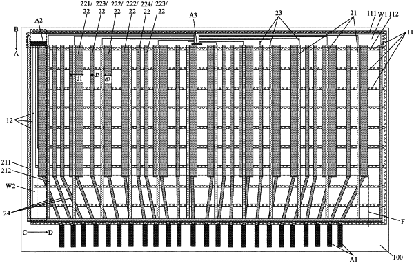
1. A light emitting substrate, comprising: a base substrate, and an electrode layer, a first insulating layer, a first wiring layer, a second insulating layer, a second wiring layer and light emitting elements sequentially located on a side of the base substrate; wherein
the electrode layer comprises: a plurality of first touch control electrodes extending along a first direction;
the first wiring layer comprises: a plurality of driving signal wires extending along a second direction and configured to drive the light emitting elements to emit light, and a plurality of second touch control electrodes extending along the second direction, wherein the second touch control electrodes are insulated from the first touch control electrodes, and the second direction intersects with the first direction; and
the second wiring layer comprises: connection signal wires configured to connect different light emitting elements;
wherein the light emitting substrate further comprises first fanout wires in a one-to-one correspondence with the driving signal wires, one ends of the first fanout wires are connected with the driving signal wires, and the other ends of the first fanout wires are connected to first terminals; and
the light emitting substrate further comprises second fanout wires in a one-to-one correspondence with the first touch control electrodes, and third fanout wires in a one-to-one correspondence with the second touch control electrodes, wherein one ends of the second fanout wires are connected with the first touch control electrodes, the other ends of the second fanout wires are connected to second terminals, one ends of the third fanout wires are connected with the second touch control electrodes, the other ends of the third fanout wires are connected to third terminals, and the second terminals and the third terminals are located on a same side of the base substrate;
wherein the first terminals and the second terminals are located on opposite sides of the base substrate; and
a direction pointing from a side where the second terminals are located to a side where the first terminals are located is set as a first pointing direction, a region between a first piece of the first touch control electrodes and a second piece of the second touch control electrodes in the first pointing direction is set as a first touch control inactive region, and an orthographic projection of the first touch control inactive region on the base substrate covers a region where the third fanout wires are located.
|