| CPC G06F 3/0446 (2019.05) [G03F 7/092 (2013.01); G06F 3/0443 (2019.05); G06F 3/0445 (2019.05); H10K 59/40 (2023.02); G06F 2203/04102 (2013.01); G06F 2203/04103 (2013.01); G06F 2203/04111 (2013.01); G06F 2203/04112 (2013.01); Y10T 29/49117 (2015.01)] | 6 Claims |
|
1. A method of manufacturing a touch panel, comprising:
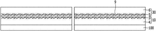
forming a first photosensitive conductive layer, which comprises a first photosensitive resin layer and a first metal nanowire layer buried at an upper portion of the first photosensitive resin layer, over a substrate;
forming a second photosensitive conductive layer, which comprises a second photosensitive resin layer and a second metal nanowire layer buried at an lower portion of the second photosensitive resin layer, over the first photosensitive conductive layer, wherein photosensitivities of the first and second photosensitive conductive layers have opposite signs;
forming a preliminary conductive pattern by patterning the second photosensitive conductive layer and the first photosensitive conductive layer such that the first photosensitive conductive layer and the second photosensitive conductive layer have a same pattern in a plan view, such that a first sidewall of the first photosensitive conductive layer is aligned with a second sidewall of the second photosensitive conductive layer; and
forming i) a touch electrode in a touch area of the substrate and ii) a connecting wire outside of the touch area and electrically connected to the touch electrode by removing at least a portion of the second photosensitive conductive layer formed in the touch area through exposure and development of the preliminary conductive pattern.
|