| CPC G06F 3/04166 (2019.05) [G06F 3/0412 (2013.01); G06F 3/0443 (2019.05); G06F 3/0446 (2019.05); G06F 3/0448 (2019.05); G06F 3/04164 (2019.05); G06F 2203/04112 (2013.01)] | 13 Claims |
|
1. A display device comprising:
a display portion including a plurality of transistors, a plurality of organic EL elements, and a scan line; and
a capacitive touch sensor over the display portion, the capacitive touch sensor including a first conductive layer and a second conductive layer,
wherein:
the scan line is electrically connected to the plurality of transistors,
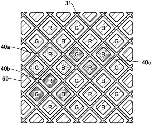
the first conductive layer has a lattice shape with a plurality of openings,
one of the plurality of organic EL elements emitting blue light is in one of the plurality of openings in a plan view,
the lattice shape has a linear portion,
an angle between a first extending direction of the linear portion of the lattice shape and a second extending direction of the scan line is greater than or equal to 30° and smaller than or equal to 60°, and
in a plan view of the display portion, a line connecting two diagonally-opposed corners of the one of the plurality of openings of the first conductive layer is aligned with a line connecting two diagonally-opposed corners of the one of the plurality of organic EL elements emitting blue light and is substantially parallel to the second extending direction.
|