US 11,747,744 B2
Electrostatic charge image developing carrier, electrostatic charge image developer, and image forming apparatus
Jumpei Iwasaki, Minamiashigara (JP); Yasuo Kadokura, Minamiashigara (JP); Shintaro Anno, Minamiashigara (JP); Kazutsuna Sasaki, Minamiashigara (JP); and Satoshi Miura, Minamiashigara (JP)
Assigned to FUJIFILM Business Innovation Corp., Tokyo (JP)
Filed by FUJIFILM Business Innovation Corp., Tokyo (JP)
Filed on Jul. 31, 2020, as Appl. No. 16/944,975.
Claims priority of application No. 2020-034173 (JP), filed on Feb. 28, 2020; application No. 2020-034174 (JP), filed on Feb. 28, 2020; and application No. 2020-034176 (JP), filed on Feb. 28, 2020.
Prior Publication US 2021/0278773 A1, Sep. 9, 2021
This patent is subject to a terminal disclaimer.
Int. Cl. G03G 9/083 (2006.01); G03G 9/097 (2006.01); G03G 15/08 (2006.01); G03G 9/08 (2006.01); G03G 9/087 (2006.01)
CPC G03G 9/0839 (2013.01) [G03G 9/0819 (2013.01); G03G 9/0825 (2013.01); G03G 9/08755 (2013.01); G03G 9/09725 (2013.01); G03G 15/08 (2013.01)] 16 Claims
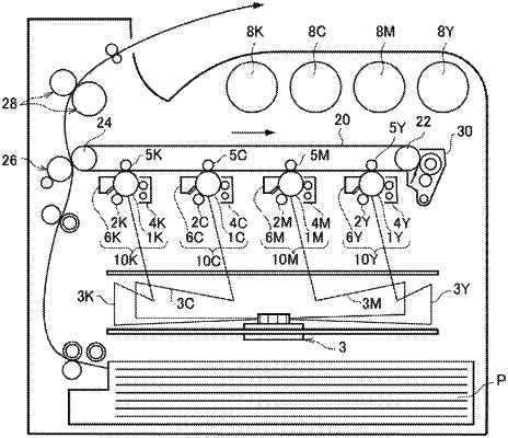
OG exemplary drawing
 
1. An electrostatic charge image developing carrier comprising:
magnetic particles; and
an acrylate resin layer coating the magnetic particles and containing silica particles,
wherein an average particle diameter of the silica particles is 5 nm or more and 90 nm or less,
wherein an average thickness of the resin layer is 0.6 μm or more and 1.4 μm or less, and
wherein a ratio B/A of a surface area B of the electrostatic charge image developing carrier to a plan view area A of the electrostatic charge image developing carrier is 1.020 or more and 1.100 or less when a surface of the electrostatic charge image developing carrier is three-dimensionally analyzed.