| CPC G02F 1/225 (2013.01) [G02F 1/0018 (2013.01); G02F 1/0316 (2013.01); G02F 1/0152 (2021.01)] | 12 Claims |
|
1. A method of manufacturing an electro-optical modulator assembly, the method comprising:
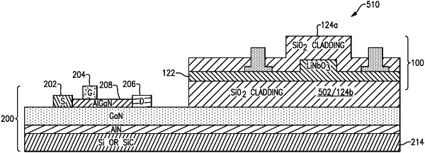
providing a transistor including a gate, a drain, and a source disposed on a first substrate;
providing a photonic modulator including a first waveguide structure positioned between a first electrode and a second electrode, the photonic modulator being disposed on a second substrate;
depositing a first oxide layer over the gate, the drain, and the source of the transistor; and
bonding the first oxide layer of the transistor to a second oxide layer of the photonic modulator such that the photonic modulator is integrated with the transistor on the first substrate and the photonic modulator is disposed over a film forming a channel layer for the transistor, the photonic modulator occupying an area that is non-overlapping with an area occupied by the transistor.
|