| CPC G02F 1/1368 (2013.01) [G02F 1/136286 (2013.01)] | 18 Claims |
|
1. A display device comprising:
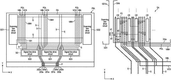
a display area where a plurality of pixels including switching elements and memories connected to the switching elements are arrayed;
a first drive circuit arranged adjacent to the display area in a first direction, the first drive circuit configured to supply a drive signal to a gate electrode included in each of the switching elements;
a memory power line extending in a second direction intersecting the first direction in the display area and configured to supply a potential to the memories;
a plurality of second drive circuits supplying pixel signals to the memories; and
an input terminal connected to an end portion of the memory power line,
wherein
an outer edge of the display area is defined by outermost edges of the pixels located on an outermost side in the display area,
a first distance from the first drive circuit to the outer edge of the display area is shorter than a second distance from the first drive circuit to the memory power line,
the input terminal and the display area are arranged in the second direction with a certain distance therebetween,
the plurality of second drive circuits are arranged in the first direction at positions between the display area and the input terminal, and
the memory power line passes through a region between two of the second drive circuits, from the input terminal to the display area.
|