| CPC G02F 1/136286 (2013.01) [G02F 1/133548 (2021.01)] | 17 Claims |

|
1. A display assembly, comprising:
a first substrate and a second substrate that are disposed opposite;
a first liquid crystal layer located between the first substrate and the second substrate;
a third substrate disposed at a side of the first substrate away from the second substrate;
a second liquid crystal layer located between the first substrate and the third substrate;
a first pixel circuit layer disposed between the first substrate and the first liquid crystal layer;
a second pixel circuit layer disposed between the third substrate and the second liquid crystal layer;
a polarizing device disposed on a side of the second pixel circuit layer away from the second liquid crystal layer; and
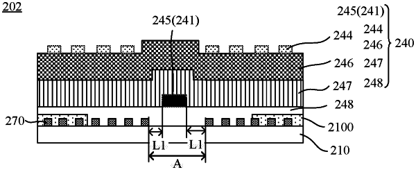
a first metal wire grid polarizing layer disposed between the first substrate and the first pixel circuit layer, the first metal wire grid polarizing layer being electrically insulated from the first pixel circuit layer; wherein
the first pixel circuit layer includes at least one first signal line;
the first metal wire grid polarizing layer includes at least one first discontinuous region each extending in an extending direction of a first signal line, and an orthogonal projection of the first signal line on the first substrate and an orthogonal projection of a first discontinuous region on the first substrate have an overlapping region;
borders of the orthogonal projection of the first signal line on the first substrate that extend in the extending direction of the first signal line are within borders of the orthogonal projection of the first discontinuous region on the first substrate that extend in an extending direction of the first discontinuous region; and
in a width direction of the first signal line, a gap exists between a border of the orthogonal projection of the first signal line on the first substrate that extends in the extending direction of the first signal line and a border, close to the border of the orthogonal projection of the first signal line, of the orthogonal projection of the first discontinuous region on the first substrate that extends in the extending direction of the first discontinuous region.
|