| CPC G02F 1/136213 (2013.01) [G02F 1/133512 (2013.01); G02F 1/133388 (2021.01)] | 11 Claims |
|
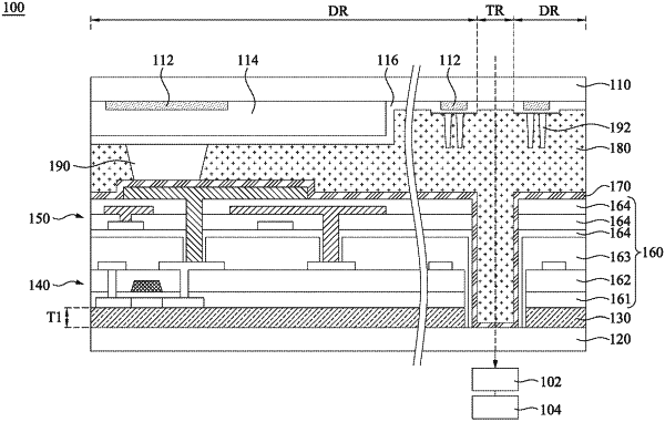
1. An electronic device, comprising:
a first substrate comprising a transmitting region, a display region, and a periphery region, wherein the periphery region surrounds the display region, and the display region surrounds the transmitting region;
a second substrate disposed opposite to the first substrate;
a buffer layer disposed on the second substrate;
a protection layer disposed on the buffer layer;
an active array disposed on the buffer layer;
a pixel array disposed on the active array and electrically connected to the active array; and
an alignment film conformally disposed on the protection layer and the second substrate, wherein the alignment film comprises a first portion in direct contact with the second substrate, and a vertical projection of the first portion of the alignment film overlaps the transmitting region of the first substrate.
|