| CPC G02F 1/13452 (2013.01) [G02F 1/13336 (2013.01); G02F 1/136286 (2013.01); H01L 27/124 (2013.01); H01L 27/1259 (2013.01); H05K 1/189 (2013.01); H05K 3/303 (2013.01); G02F 1/136295 (2021.01); H05K 2201/10136 (2013.01); H05K 2203/107 (2013.01)] | 20 Claims |
|
1. A display device comprising:
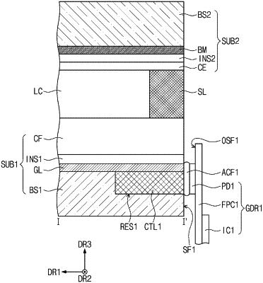
a first base substrate;
a second base substrate overlapping the first base substrate;
an image display layer disposed between the first base substrate and the second base substrate;
a gate driver disposed at a first side surface of the first base substrate;
a data driver disposed at a second side surface of the first base substrate;
first conductive layers respectively disposed in first recesses recessed from the first side surface of the first base substrate;
gate lines extending lengthwise individually in the first direction, overlapping the first base substrate, separate from the first conductive layers, disposed on the first conductive layers, and respectively electrically connected to the first conductive layers;
data lines extending lengthwise individually in the second direction, electrically insulated from the gate lines, and overlapping the first base substrate; and
pixels electrically connected to the gate lines and the data lines,
wherein a first recess among the first recesses comprises three flat faces formed of a same material,
wherein a first conductive layer among the first conductive layers directly contacts each of the three flat faces and directly contacts a flat contact face of a gate line among the gate lines,
wherein the gate driver comprises first pads and a first driving chip electrically connected through the first pads to the first conductive layers, and
wherein a first pad among the first pads overlaps a flat contact face of the first conductive layer exposed through the first side surface of the first base substrate.
|