| CPC G02F 1/1345 (2013.01) | 15 Claims |
|
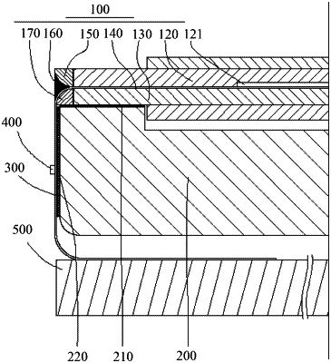
1. A display panel, comprising a first substrate, on which a conductive structure layer is formed, wherein:
the conductive structure layer has a bonding area close to a side edge thereof, at least a part of the bonding area of the conductive structure layer protrudes from a first side edge of the first substrate, and is bent toward a side of the first substrate away from the conductive structure layer and fixed;
an end surface of the first side edge of the first substrate is provided with a first protective strip, the first protective strip has a first smooth surface facing the conductive structure layer and smoothly connected with a side surface of the first substrate on which the conductive structure layer is formed, and a bent part of the conductive structure layer is attached to the first smooth surface and
the display panel further comprises a second substrate covering on the conductive structure layer, wherein an end surface of the second substrate corresponding to the end surface of the first side edge of the first substrate is provided with a second protective strip, and a fixing adhesive is filled between the second protective strip and the bent part of the conductive structure layer.
|