| CPC G02F 1/134309 (2013.01) [G02F 1/13439 (2013.01); G02F 1/133514 (2013.01); G02F 1/136222 (2021.01); G02F 1/136286 (2013.01); G02F 2201/123 (2013.01)] | 5 Claims |
|
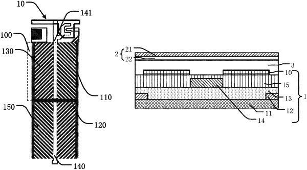
1. A display panel, comprising:
an array substrate and a color film substrate disposed opposite to each other; and
liquid crystals filled between the array substrate and the color film substrate,
wherein the array substrate comprises:
a base substrate;
a first common electrode disposed on a surface of a side of the base substrate;
an insulating layer disposed on the surface of the side of the base substrate and covering the first common electrode;
a data line disposed on a surface of a side of the insulating layer away from the base substrate;
a color resist layer disposed on a surface of a side of the data line and the insulating layer away from the base substrate; and
a pixel electrode formed on a surface of a side of the color resist layer away from the insulating layer;
wherein the pixel electrode comprises:
a stripe main electrode, wherein the stripe main electrode comprises a first main electrode and a second main electrode, the first main electrode comprises two main traces parallel to a first direction, the second main electrode is disposed along a second direction, and the second main electrode is disposed between the two main traces parallel to the first direction;
a first metal trace disposed along the first direction, wherein the first metal trace is disposed between the two main traces parallel to the first direction and is coupled to the first main electrode and the second main electrode to form four display regions; and
a plurality of branch electrodes arranged at intervals in the four display region;
wherein the data line is disposed right under the first metal line and a width of the data line ranges from 6.5 μm to 7.5 μm;
wherein the first common electrode is disposed at an edge of the base substrate, and a width of the first common electrode ranges from 2.5 μm to 3 μm;
wherein a cross-sectional width of a part where an orthographic projection of the pixel electrode projected on the base substrate overlaps with the first common electrode ranges from 0.5 μm to 1 μm.
|