| CPC G02F 1/133385 (2013.01) [E06B 9/24 (2013.01); G02F 1/13306 (2013.01); G02F 1/13338 (2013.01); G02F 1/133382 (2013.01); G02F 1/133601 (2021.01); H01L 23/38 (2013.01); H10N 10/17 (2023.02); G02F 2203/69 (2013.01)] | 16 Claims |
|
1. A windowing device, comprising:
a windowing module comprising a dimming transparent substrate and a semiconductor temperature adjustment element arranged on the dimming transparent substrate, the dimming transparent substrate being provided with different light transmittances when the dimming transparent substrate has different adjustment parameters;
a temperature adjustment circuitry coupled to the semiconductor temperature adjustment element, and configured to input a current to the semiconductor temperature adjustment element and adjust a temperature of the semiconductor temperature adjustment element;
a temperature sensor arranged on the windowing module and configured to detect a temperature of an environment where the windowing module is located; and
a controller coupled to the temperature sensor and the temperature adjustment circuitry, and configured to input a circuitry adjustment signal to the temperature adjustment circuitry when the temperature detected by the temperature sensor is beyond a predetermined temperature range, so that the temperature adjustment circuitry adjusts the current inputted to the semiconductor temperature adjustment element in such a manner as to adjust a temperature of the dimming transparent substrate to be within the predetermined temperature range through adjusting the temperature of the semiconductor temperature adjustment element;
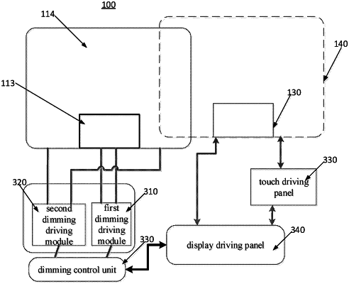
wherein the windowing module further comprises a transparent display panel arranged opposite to the dimming transparent substrate, and an orthogonal projection of the transparent display panel onto a plane where the dimming transparent substrate is located is completely within the dimming transparent substrate; and
the windowing module further comprises a touch panel arranged at a side of the transparent display panel away from the dimming transparent substrate, an orthogonal projection of the touch panel onto the plane where the dimming transparent substrate is located covers the entire dimming transparent substrate, and the orthogonal projection of transparent display panel onto the plane where the dimming transparent substrate is located covers a part of the dimming transparent substrate.
|