| CPC G02B 6/1228 (2013.01) [G02B 6/125 (2013.01); G02B 6/136 (2013.01); G02B 2006/12061 (2013.01)] | 15 Claims |
|
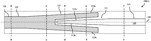
12. A structure comprising:
a first waveguide with a first main body and a first end portion, wherein the first end portion is a tapered end portion; and
a second waveguide with a second main body and a second end portion,
wherein the second end portion has two branch waveguides that branch out from the second main body,
wherein the two branch waveguides of the second end portion of the second waveguide are adjacent to the first end portion of the first waveguide, at opposing sides thereof respectively,
wherein the first waveguide and the second waveguide are discrete waveguides with bottom surfaces at different heights above a substrate and are physically separated from each other by at least one cladding material layer,
wherein the at least one cladding material layer includes a silicon nitride layer stacked between two silicon dioxide layers, and
wherein the first end portion of the first waveguide is below the second end portion of the second waveguide and laterally aligned between the two branch waveguides of the second end portion of the second waveguide.
|