| CPC G02B 6/12019 (2013.01) [G01J 1/58 (2013.01); G01M 11/35 (2013.01); G02B 6/12016 (2013.01); G01J 9/00 (2013.01); G02B 6/13 (2013.01)] | 18 Claims |
|
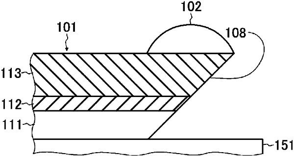
1. A wavelength checker comprising:
an optical waveguide chip; and
an optical converter comprising a conversion material configured to convert near-infrared light into visible light;
wherein the optical waveguide chip on a side connected to an optical fiber includes an arrayed waveguide grating and is mounted on a main substrate;
wherein a light emitting-side end surface of the optical waveguide chip on a side from which light is output to an external space is a reflection surface inclined to face the main substrate; and
the optical converter is provided at a location, on the optical waveguide chip, from which light reflected on the light emitting-side end surface is output to the external space.
|