| CPC G02B 6/12004 (2013.01) [G02B 6/124 (2013.01); G02B 2006/12061 (2013.01); G02B 2006/12107 (2013.01); G02B 2006/12121 (2013.01); G02B 2006/12123 (2013.01)] | 19 Claims |
|
1. An integrated circuit (IC) device comprising:
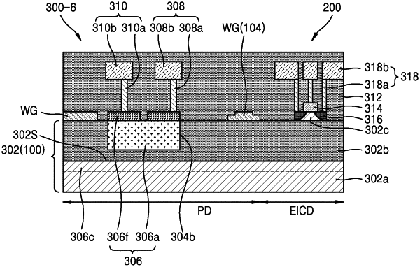
an optical IC substrate including a first silicon layer and a buried insulating layer, the buried insulating layer being on and having a bottom surface in contact with the uppermost surface of the first silicon layer;
a local trench formed within the buried insulating layer; and
a photoelectronic element including a photoelectric conversion layer formed within the local trench, the photoelectric conversion layer being spaced apart from the first silicon layer of the optical IC substrate by the buried insulating layer; and
an optical waveguide core layer,
wherein a top surface of the photoelectric conversion layer is at a lower level than a first top surface of the optical waveguide core layer in a vertical direction on the optical IC substrate, and the photoelectric conversion layer is formed to extend over a second top surface of the optical waveguide core layer.
|