| CPC G02B 6/06 (2013.01) [G02B 6/02052 (2013.01)] | 19 Claims |
|
1. An electronic device, comprising:
a display configured to produce an image; and
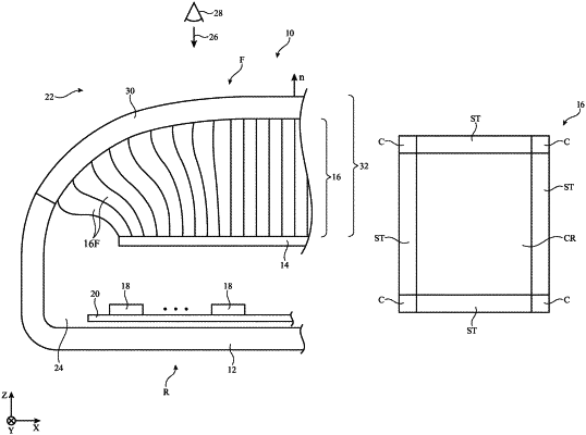
an image transport layer configured to receive the image at an input surface and to transport the received image to an output surface, wherein the image transport layer has a central portion and a peripheral portion that runs along a peripheral edge of the central portion, wherein the peripheral portion and the central portion are characterized by an elastic modulus, wherein the elastic modulus has a first modulus value in the peripheral portion and a second modulus value in the central portion, and wherein the first modulus value is less than the second modulus value, wherein the central portion includes a plurality of window portions and a surrounding portion that surrounds the plurality of window portions, wherein the plurality of window portions and the surrounding portion are characterized by a property, and wherein the property has a first value in the plurality of window portions and a second value in the surrounding portion that is different than the first value.
|