US 11,747,531 B2
Display substrate, fine metal mask set and manufacturing method thereof
Fengli Ji, Beijing (CN); Chang Luo, Beijing (CN); Jianpeng Wu, Beijing (CN); and Lujiang Huangfu, Beijing (CN)
Assigned to Chengdu BOE Optoelectronics Technology Co., Ltd., Sichuan (CN); and BOE TECHNOLOGY GROUP CO., LTD., Beijing (CN)
Filed by Chengdu BOE Optoelectronics Technology Co., Ltd., Sichuan (CN); and BOE TECHNOLOGY GROUP CO., LTD., Beijing (CN)
Filed on Aug. 4, 2022, as Appl. No. 17/880,874.
Application 17/880,874 is a continuation of application No. 16/755,970, granted, now 11,448,807, previously published as PCT/CN2019/086875, filed on May 14, 2019.
Application 16/755,970 is a continuation in part of application No. 16/234,777, filed on Dec. 28, 2018, granted, now 10,854,684, issued on Dec. 1, 2020.
Application 16/234,777 is a continuation in part of application No. 15/578,481, abandoned, previously published as PCT/CN2017/075957, filed on Mar. 8, 2017.
Application 16/234,777 is a continuation in part of application No. 15/536,347, granted, now 10,274,654, issued on Apr. 30, 2019, previously published as PCT/CN2016/081097, filed on May 5, 2016.
Claims priority of application No. 201620127445.0 (CN), filed on Feb. 18, 2016; application No. 201610585894.4 (CN), filed on Jul. 22, 2016; application No. 201810135947.1 (CN), filed on Feb. 9, 2018; application No. 201810135948.6 (CN), filed on Feb. 9, 2018; application No. 201810136335.4 (CN), filed on Feb. 9, 2018; application No. 201810137012.7 (CN), filed on Feb. 9, 2018; application No. 201810137014.6 (CN), filed on Feb. 9, 2018; application No. 201810137016.5 (CN), filed on Feb. 9, 2018; and application No. 201811525578.3 (CN), filed on Dec. 13, 2018.
Prior Publication US 2022/0381957 A1, Dec. 1, 2022
Int. Cl. G02B 5/20 (2006.01); G09F 9/33 (2006.01); G09F 9/302 (2006.01); G02F 1/1343 (2006.01); G02F 1/136 (2006.01); G02F 1/1362 (2006.01); H10K 59/35 (2023.01)
CPC G02B 5/201 (2013.01) [G02F 1/136 (2013.01); G02F 1/1362 (2013.01); G02F 1/134309 (2013.01); G09F 9/302 (2013.01); G09F 9/3023 (2013.01); G09F 9/33 (2013.01); H10K 59/353 (2023.02); G02F 1/134345 (2021.01)] 20 Claims
OG exemplary drawing
 
1. A display substrate, comprising:
a base substrate; and
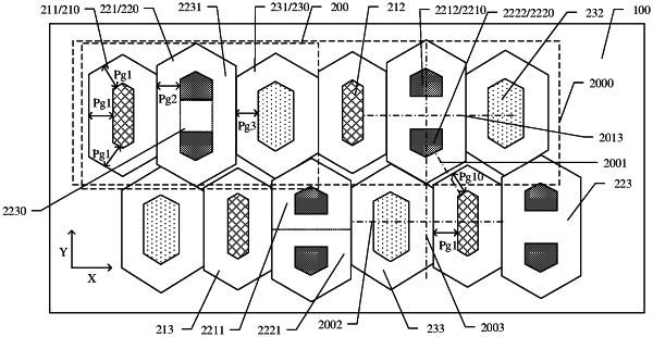
a plurality of repeat units on the base substrate, wherein each of the plurality of repeat units comprises one first-color sub-pixel, two second-color sub-pixels and one third-color sub-pixel, in at least one of the plurality of repeat units, the one first-color sub-pixel and the one third-color sub-pixel are arranged in a first direction, the two second-color sub-pixels are arranged in a second direction, the plurality of repeat units are arranged in the first direction to form a plurality of repeat unit groups, the plurality of repeat unit groups are arranged in the second direction, and adjacent repeat unit groups in the plurality of repeat unit groups are staggered from each other in the first direction,
wherein each of the one first-color sub-pixel, the two second-color sub-pixels and the one third-color sub-pixel comprises a light-emitting layer, and light-emitting layers of at least two adjacent sub-pixels of different colors in the first direction are connected with each other;
in three sub-pixels of different colors which are adjacent to each other and located in two adjacent repeat unit groups, light-emitting layers of at least two sub-pixels adjacent to each other are connected with each other, and a spacing is disposed between at least part of the light-emitting layers of two sub-pixels which are adjacent to each other and located in different repeat unit groups.