| CPC G02B 5/1866 (2013.01) [G02B 1/115 (2013.01); G02B 1/14 (2015.01); G02B 5/1847 (2013.01); G01S 7/4811 (2013.01)] | 15 Claims |
|
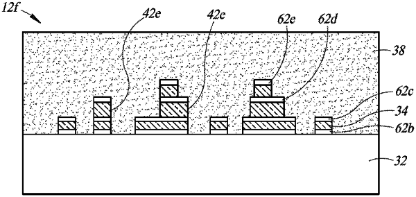
1. A lens, comprising:
a substrate;
a plurality of microstructures on the substrate, the plurality of microstructures having a plurality of different heights and widths, each of the plurality of microstructures including;
a plurality of portions of a first material having a first refractive index; and
a plurality of coatings that are optical filter coatings or anti-reflective coatings, the plurality of portions being spaced apart from the substrate by one of the plurality of coatings, each of the plurality of portions being spaced from another portion of the plurality of portions by a respective coating of the plurality of coatings; and
a protective layer on the plurality of microstructures, the protective layer being a second material having a second refractive index that is different from the first refractive index.
|