US 11,747,528 B2
Diffraction grating device, method of manufacturing the same, and optical apparatus including the diffraction grating device
Brandon Born, Stanford, CA (US); Mark L. Brongersma, Stanford, CA (US); and Sunghoon Lee, Seoul (KR)
Assigned to SAMSUNG ELECTRONICS CO., LTD., Suwon-si (KR); and The Board of Trustees of the Leland Stanford Junior University, Stanford, CA (US)
Filed by SAMSUNG ELECTRONICS CO., LTD., Suwon-si (KR); and The Board of Trustees of the Leland Stanford Junior University, Stanford, CA (US)
Filed on Aug. 30, 2019, as Appl. No. 16/557,421.
Claims priority of provisional application 62/725,868, filed on Aug. 31, 2018.
Claims priority of application No. 10-2018-0141133 (KR), filed on Nov. 15, 2018.
Prior Publication US 2020/0073031 A1, Mar. 5, 2020
Int. Cl. G02B 5/18 (2006.01); G02B 27/42 (2006.01); G02B 5/26 (2006.01); G02B 27/01 (2006.01); G02B 27/00 (2006.01); G02B 6/293 (2006.01)
CPC G02B 5/1847 (2013.01) [G02B 5/1819 (2013.01); G02B 5/1861 (2013.01); G02B 5/1866 (2013.01); G02B 27/0081 (2013.01); G02B 27/0101 (2013.01); G02B 27/4272 (2013.01); G02B 5/26 (2013.01); G02B 6/29308 (2013.01)] 32 Claims
OG exemplary drawing
 
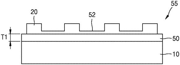
1. A diffraction grating device comprising:
a light reflection substrate; and
a diffraction grating arranged on the light reflection substrate,
wherein the diffraction grating comprises a plurality of diffraction elements, and
wherein the diffraction grating device further comprises a dielectric layer between the light reflection substrate and the diffraction grating, wherein a thickness of the dielectric layer is an integer multiple of a wavelength of light incident on the diffraction grating.