| CPC G01R 31/3177 (2013.01) [G01R 31/318541 (2013.01); G01R 31/318552 (2013.01); G01R 31/318594 (2013.01); H03K 3/0372 (2013.01); H03K 19/21 (2013.01)] | 20 Claims |
|
1. A circuit, comprising:
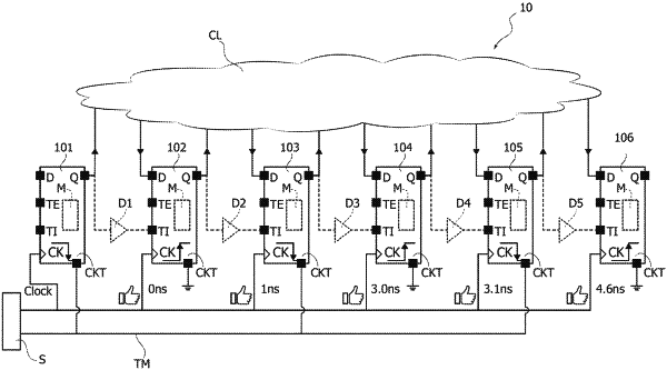
a scan chain including a plurality of flip-flops that are cascaded in a chain, each flip-flop of the plurality of flip-flops having a respective functional input node and a respective test input node, each flip-flop of the plurality of flip-flops being configured to be selectively couple the respective functional input node or the respective test input node to logic circuitry, and each flip-flop of the plurality of flip-flops being triggered by a clock edge at a clock edge time; and
clock circuitry configured to output at least one clock signal to the plurality of flip-flops, wherein active clock edges are applied to the plurality of flip-flops at respective clock edge times,
wherein the plurality of flip-flops include a set of flip-flops configured to:
receive an edge inversion signal; and
selectively invert the active clock edges in response to the edge inversion signal being asserted.
|