| CPC G01N 33/497 (2013.01) [G01N 27/04 (2013.01); G01N 27/12 (2013.01); G01N 2033/4975 (2013.01); G01N 2800/122 (2013.01)] | 39 Claims |
|
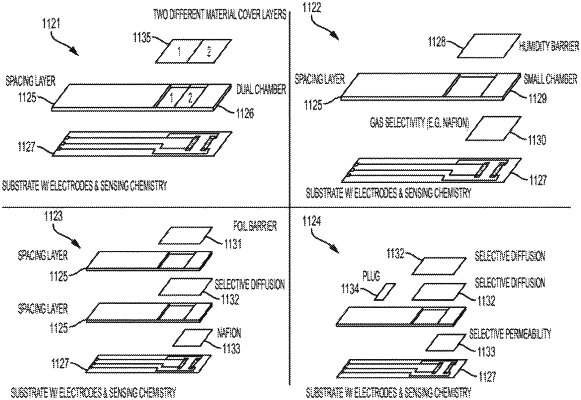
1. A test strip comprising:
a flexible substrate layer;
a first electrode pair disposed upon the flexible substrate layer;
at least one sensing chemistry selected based on an analyte of interest, the sensing chemistry being disposed upon at least a portion of the substrate layer, and the sensing chemistry being disposed upon at least a portion of the first electrode pair, wherein the sensing chemistry comprises functionalized nanostructures to bind to an analyte causing at least one of an electrical resistance change across the nanostructures and a redox reaction at the nanostructures;
at least one flexible spacing layer, the at least one flexible spacing layer disposed upon at least a portion of the flexible substrate layer, and the at least one flexible spacing layer disposed upon at least a portion of the first electrode pair, and wherein the flexible spacing layer is not in contact with at least a portion of the sensing chemistry; and
a flexible protective layer disposed above the flexible spacing layer, wherein the flexible protective layer is not in contact with at least a portion of the sensing chemistry, wherein the flexible protective layer is impermeable to at least the analyte of interest; and
wherein at least a portion of the flexible substrate layer, at least a portion of the at least one flexible spacing layer, and at least a portion of the flexible protective layer define a chamber enclosing at least a portion of the functionalized nanostructures.
|