| CPC G01N 21/7703 (2013.01) [B01L 3/502715 (2013.01); G01N 33/54373 (2013.01)] | 18 Claims |

|
1. A test apparatus, comprising:
a test card having a coupling end; and
a test structure located on the test card, comprising:
a silicon substrate;
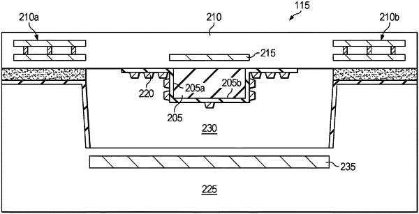
a planar waveguide formed on the silicon substrate and having an uncladded sensor portion comprising an outer surface and side surfaces, wherein the silicon substrate comprises a semiconductor material;
nanoparticles located on the outer surface and on the side surfaces of the uncladded sensor portion of the planar waveguide, wherein a concentration of the nanoparticles is higher on the side surfaces of the planar waveguide than on the outer surface;
a fluid input port located over the planar waveguide and in fluid communication with the planar waveguide that allows an analyte deposited into the fluid input port to contact the planar waveguide; and
an optical output end that includes optical fibers located within v-grooves on the silicon substrate that are optically coupled to the planar waveguide and extend to the coupling end of the test card.
|