| CPC G01N 1/286 (2013.01) [G01N 2001/2873 (2013.01)] | 12 Claims |
|
1. A method of producing a test-sample for a transmission electron microscope, comprising:
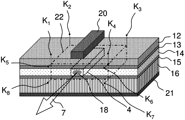
a process step of cutting out, from a laser diode being a workpiece, a massive body in a rectangular parallelepiped shape including a multiple quantum well active layer residing in the laser diode;
a process step of producing a test-sample in which tilting oblique cutoff portions are formed, at two corner portions contiguously bordering on an upper surface of the massive body, each tilting with respect to the upper surface of the massive body;
a process step of making the test-sample thinner by working on the test-sample from a surface thereof until a thickness thereof reaches where the multiple quantum well active layer therein can be observed; and
a process step of cutting out an observation test-sample being columnar, from a test-sample formed with the tilting oblique cutoff portions, by using two of surface-part active layers each made of portions of the multiple quantum well active layer.
|