| CPC G01J 1/44 (2013.01) [G01J 1/0425 (2013.01); G06F 1/10 (2013.01); H10N 60/84 (2023.02); G01J 2001/442 (2013.01)] | 20 Claims |
|
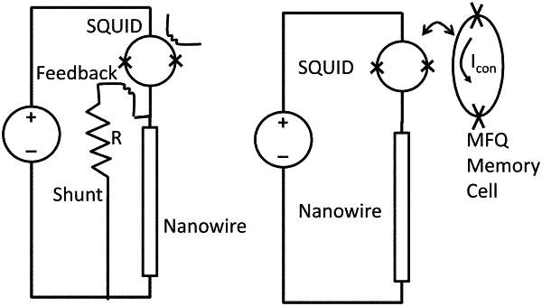
1. A nanowire photon detector, comprising:
an integral substrate;
at least one superconducting nanowire configured to absorb a photon emitted from a photon source, the at least one superconducting nanowire being supported by the integral substrate;
an electrical current bias source, coupled to the at least one nanowire, configured to generate a bias current on the at least one superconducting nanowire, wherein absorption of the photon by the at least one superconducting nanowire subject to the bias current generates a voltage pulse along the at least one superconducting nanowire; and
at least one superconducting Josephson junction circuit having a logic state, formed at least partially on the integral substrate, electrically connected with the at least one superconducting nanowire, and being configured to:
receive the voltage pulse;
control a bias current of the electrical bias current source below a critical current of the at least one superconducting nanowire; and
produce a changed logic state of the at least one superconducting Josephson junction circuit dependent on receipt of the generated voltage pulse.
|