| CPC G01J 1/44 (2013.01) [G01S 7/4816 (2013.01); G01S 7/4876 (2013.01); G01S 7/493 (2013.01); H01L 27/1446 (2013.01); G01J 2001/448 (2013.01); G01J 2001/4466 (2013.01)] | 10 Claims |
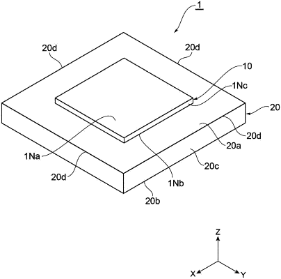
|
1. A light detection device, comprising:
a light detection substrate that includes a semiconductor substrate including a first main surface and a second main surface opposite to each other, and a light detection region provided with a plurality of pixels, the plurality of pixels two-dimensionally arranged when viewed from a direction orthogonal to the first main surface; and
a circuit substrate that is connected to the light detection substrate in a direction orthogonal to the first main surface and includes a signal processing region provided with a plurality of signal processing units, the plurality of signal processing units each being configured to process a detection signal output from a corresponding one of the pixels,
wherein for each of the pixels, the light detection substrate includes,
a plurality of avalanche photodiodes, each of which includes a light-receiving region provided in the semiconductor substrate and is arranged to operate in Geiger mode,
a plurality of quenching resistors, each of which is electrically connected to a corresponding one of the avalanche photodiodes in series, and
a pad electrode to which the plurality of quenching resistors are electrically connected in parallel,
a plurality of the light-receiving regions of the plurality of avalanche photodiodes are two-dimensionally arranged for each of the pixels when viewed from a direction orthogonal to the first main surface,
each of the plurality of the signal processing units includes,
a signal acquisition unit configured to acquire the detection signal through a corresponding pad electrode, the corresponding pad electrode corresponding to the pad electrode,
a timing measurement unit configured to measure timing at which light is incident on a corresponding one of the pixels, based on the detection signal,
an energy measurement unit configured to measure energy of the light incident on a corresponding one of the pixels, based on the detection signal, and
a storage unit configured to store a measurement result in the timing measurement unit and the energy measurement unit, and
the light detection region and the signal processing region overlap each other at least at a part when viewed from a direction orthogonal to the first main surface.
|