| CPC C23C 14/042 (2013.01) [C23C 14/588 (2013.01); C23C 14/5813 (2013.01); H10K 71/166 (2023.02)] | 4 Claims |
|
1. A vapor deposition mask comprising:
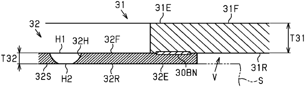
a sheet-shaped mask portion made of an iron-nickel alloy and having a contact surface, which is configured to be in contact with a vapor deposition target, and a non-contact surface, which is opposite to the contact surface, wherein the mask portion includes a plurality of mask holes each extending from a first opening, which is located in the non-contact surface, to a second opening, which is located in the contact surface, and the second opening is smaller in size than the first opening; and
a mask frame that has a welding mark welded to the non-contact surface, has a higher rigidity than the mask portion, and is in a shape of a frame surrounding the mask holes,
the mask portion is formed by peeling off a plastic layer and a glass substrate from the mask portion after making the welding mark in a state where the glass substrate is joined to the contact surface with the plastic layer,
the welding mark is located on the non-contact surface opposite to the contact surface that follows the surface of the glass substrate.
|