| CPC A61B 5/686 (2013.01) [A61B 5/0245 (2013.01); A61N 1/05 (2013.01); A61N 1/372 (2013.01); A61N 1/3754 (2013.01); H05K 1/115 (2013.01); H05K 1/183 (2013.01); H05K 3/0017 (2013.01); H05K 3/32 (2013.01); H05K 3/4038 (2013.01); H05K 5/0247 (2013.01); H05K 5/03 (2013.01); H05K 5/066 (2013.01); H05K 5/069 (2013.01); A61N 1/37512 (2017.08); A61N 2001/37294 (2013.01); H05K 2201/09036 (2013.01)] | 20 Claims |
|
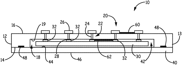
1. A medical device comprising a hermetically-sealed package, the package comprising:
a non-conductive substrate comprising a first major surface, a second major surface, and a cavity disposed in the first major surface, wherein the cavity comprises a recessed surface;
a cover layer disposed over the cavity and attached to the first major surface of the non-conductive substrate to form a hermetically-sealed enclosure, wherein the cover layer is attached to the first major surface of the non-conductive substrate by a laser bond that includes a bond line;
a feedthrough comprising:
a via between the recessed surface of the cavity and the second major surface of the substrate;
a conductive material disposed in the via; and
an external contact disposed over the via on the second major surface of the non-conductive substrate, wherein the external contact is electrically connected to the conductive material disposed in the via, and wherein the external contact is hermetically sealed to the second major surface of the non-conductive substrate by a laser bond surrounding the via; and
an electronic device disposed within the hermetically-sealed enclosure, wherein the electronic device comprises a device contact that is electrically connected to the conductive material disposed in the via such that the electronic device is electrically connected to the external contact.
|