| CPC H10N 60/83 (2023.02) [C23C 16/45536 (2013.01); H01L 29/0669 (2013.01); H10N 60/0801 (2023.02)] | 20 Claims |
|
1. A method of fabricating a device, comprising:
providing a substrate defining a plane;
forming portions of electronic circuitry over the substrate;
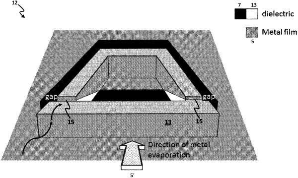
forming a shadow wall structure over the substrate; and
after forming said portions and the shadow walls, depositing an upper conducting layer over the substrate by angled deposition of a conducting material in at least a first deposition direction at an acute angle to the plane of the substrate, wherein the shadow wall structure is arranged to cast a shadow in the deposition, leaving areas where the conducting material is not deposited;
wherein the shadow wall structure comprises one or more gaps each shorter than a shadow length of a respective part of the shadow wall structure casting the shadow into the gap, to prevent the conducting material forming in the gaps and to thereby create regions of said upper conducting layer that are electrically isolated from one another; and
wherein said electrically isolated regions are arranged to form conducting elements for applying signals to, and/or receiving signals from, the electronic circuitry.
|