| CPC H10N 50/01 (2023.02) [H10B 61/22 (2023.02); H10N 50/10 (2023.02); H10N 50/80 (2023.02); H10N 50/85 (2023.02)] | 8 Claims |
|
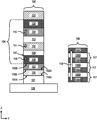
1. A memory device, comprising:
a first electrode;
a conductive layer comprising iridium and one of iron or cobalt, the conductive layer above the first electrode, wherein a concentration of the iron or the cobalt varies from an uppermost surface to a lowermost surface of the conductive layer;
a magnetic junction on the conductive layer, the magnetic junction comprising:
a magnetic structure comprising a stack of bilayers, wherein each bilayer comprises a magnetic layer and a non-magnetic layer on the magnetic layer;
a spacer layer on the magnetic structure;
a first magnet with a first magnetization on the spacer layer;
a second magnet with a second magnetization, the second magnet above the first magnet; and
a layer between the first magnet and the second magnet; and
a second electrode above the magnetic junction.
|