| CPC H10K 65/00 (2023.02) [G06V 40/1318 (2022.01); H10K 59/122 (2023.02); H10K 59/124 (2023.02); H10K 59/125 (2023.02); H10K 59/1201 (2023.02); H10K 59/40 (2023.02)] | 4 Claims |
|
1. A display substrate having a fingerprint identification region, the display substrate comprising:
a base substrate;
a display unit on the base substrate and comprising a display thin film transistor and a light-emitting device, a second electrode of the display thin film transistor being coupled to a first electrode of the light-emitting device; and
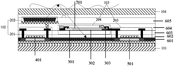
a fingerprint identification unit at a gap between adjacent display units in the fingerprint identification region and comprising a fingerprint identification transistor and a photosensitive device, a first electrode of the fingerprint identification transistor being coupled to a second electrode of the photosensitive device, wherein
the display substrate further comprises a gate insulating layer on a side of an active layer of the display thin film transistor and an active layer of the fingerprint identification transistor distal to the base substrate,
an interlayer insulating layer on a side of the gate insulating layer distal to the base substrate and covering a gate electrode of the display thin film transistor and a gate electrode of the fingerprint identification transistor, and
an interlayer dielectric layer on a side of the interlayer insulating layer distal to the base substrate,
wherein the photosensitive device is a planar PIN photodiode and comprises a P-type semiconductor layer, an I-type semiconductor layer, and an N-type semiconductor layer sequentially arranged in a first direction parallel to the base substrate and in contact with each other, and the I-type semiconductor layer is between the P-type semiconductor layer and the N-type semiconductor layer,
the I-type semiconductor layer of the photosensitive device, first and second electrodes of the display thin film transistor, and first and second electrodes of the fingerprint identification transistor are on a side of the interlayer dielectric layer distal to the base substrate,
the first electrode of the fingerprint identification transistor is coupled to the second electrode of the photosensitive device through a via hole penetrating through the interlayer dielectric layer and the interlayer insulating layer,
the photosensitive device further comprises a transparent insulating layer completely covering the P-type semiconductor layer, the I-type semiconductor layer, and the N-type semiconductor layer,
a first electrode of the photosensitive device is in contact with a side surface of the P-type semiconductor layer, and is in contact with an upper surface of the P-type semiconductor layer through a first via hole penetrating through the transparent insulating layer, and
the second electrode of the photosensitive device is in contact with a side surface of the N-type semiconductor layer, and is in contact with an upper surface of the N-type semiconductor layer through a second via hole penetrating through the transparent insulating layer.
|