| CPC H10K 59/40 (2023.02) [G06F 3/0412 (2013.01); H10K 50/84 (2023.02); H10K 59/122 (2023.02); H10K 59/1213 (2023.02); H10K 59/131 (2023.02); H10K 71/00 (2023.02)] | 20 Claims |
|
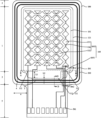
1. A display panel, comprising:
a substrate comprising:
a display region,
a peripheral region surrounding the display region, and
a pad region disposed on a side, distal from the display region, of the peripheral region,
a first dam disposed in the peripheral region and surrounding the display region;
a planarization layer disposed within the first dam, wherein a first groove is defined between the first dam and the planarization layer, and wherein an edge of a first side of the planarization layer, along an extending direction of the edge of the first side, comprises a first segment boundary and a second segment boundary that are connected, and the first side and the pad region are disposed on a same side of the display region;
a packaging layer covering the planarization layer; and
a touch layer disposed on the packaging layer, wherein the touch layer comprises a touch signal line and a touch electrode pattern, one end of the touch signal line being electrically connected to the touch electrode pattern, the other end of the touch signal line, extending from the display region to the pad region and traveling through the first segment boundary, and being electrically connected to a pad in the pad region;
wherein the packaging layer comprises an organic layer, an edge of the organic layer on a same side of the display region as the first side of the planarization layer being disposed in the first groove, and a distance between the edge of the organic layer and the first segment boundary of the planarization layer being greater than a distance between the edge of the organic layer and the second segment boundary.
|