| CPC H10K 59/124 (2023.02) [H10K 59/123 (2023.02); H10K 59/131 (2023.02); H10K 59/10 (2023.02)] | 11 Claims |
|
1. A display apparatus comprising:
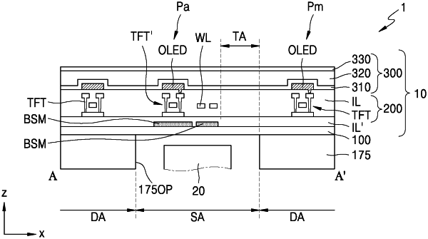
a substrate comprising a display area and a sensor area, wherein the display area comprises a first pixel, and the sensor area comprises a second pixel and a transmission portion;
a sensor configured to transceive a signal through the substrate via the transmission portion, wherein the sensor is disposed corresponding to the sensor area,
wherein the second pixel comprises an organic light-emitting diode and a first semiconductor layer, wherein the organic light-emitting diode is electrically connected to the first semiconductor layer, and
wherein a first blocking layer is disposed between the sensor and the first semiconductor layer in a direction substantially perpendicular to the substrate, wherein the first blocking layer fully covers the whole area of the first semiconductor layer in a top view of the substrate,
wherein when viewed in the direction horizontal to the substrate, the first blocking layer overlaps at least a portion of the organic light emitting diode connected to the first semiconductor layer.
|