| CPC H10K 59/122 (2023.02) [H10K 50/844 (2023.02); H10K 71/00 (2023.02); H10K 77/111 (2023.02); H10K 59/1201 (2023.02)] | 20 Claims |
|
1. A display panel, comprising:
a display substrate, comprising a flexible base substrate and comprising a plurality of light emitting elements, a pixel defining layer, and an encapsulation layer, wherein the plurality of light emitting elements, the pixel defining layer, and the encapsulation layer are on the base substrate, the pixel defining layer separates the plurality of light emitting elements, and the encapsulation layer is on a side of the plurality of light emitting elements away from the base substrate;
an optical adhesive layer, on a side of the encapsulation layer away from the base substrate; and
a cover plate, on a side of the optical adhesive layer away from the display substrate and connected with the display substrate through the optical adhesive layer,
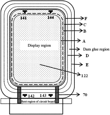
wherein the display panel comprises a display region and a frame region at a periphery of the display region;
the frame region comprises a dam glue region where an annular dam glue is located and an annular cutting region which is on a side of the dam glue away from the display region;
the encapsulation layer comprises a first inorganic encapsulation layer, a first organic encapsulation layer, and a second inorganic encapsulation layer which are sequentially arranged in a direction away from the base substrate;
the display substrate further comprises a plurality of cover plate alignment marks configured for aligning the display substrate with the cover plate; and
at least one of the plurality of cover plate alignment marks is overlapped with the second inorganic encapsulation layer in a direction perpendicular to the base substrate, and an orthographic projection of the at least one of the plurality of cover plate alignment marks on the base substrate is between an orthographic projection of dam glue on the base substrate and the display region, and/or an orthographic projection of at least one of the plurality of cover plate alignment marks on the base substrate is between the orthographic projection of the dam glue on the base substrate and the cutting region.
|