| CPC H10K 50/8426 (2023.02) [H10K 59/00 (2023.02); H10K 59/121 (2023.02); H10K 59/122 (2023.02); H10K 59/124 (2023.02); H10K 71/00 (2023.02); H10K 59/1201 (2023.02)] | 11 Claims |
|
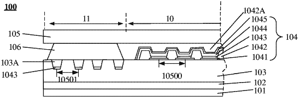
1. A substrate, comprising a display region and a peripheral region positioned in a periphery of the display region and used for sealing, the substrate comprising:
a base substrate;
an insulating layer, arranged on a side of the base substrate and positioned in the display region and the peripheral region;
a plurality of pixel units, positioned on the insulating layer corresponding to the display region;
a pixel definition layer, positioned on the insulating layer corresponding to the display region, the pixel definition layer including a plurality of pixel openings for defining the plurality of pixel units,
wherein in the peripheral region, at least one groove is disposed on a side of the insulating layer which faces away from the base substrate,
wherein the peripheral region for sealing is a sealant set region, and
each of the plurality of pixel units includes:
a light-emitting element layer, arranged on a side of the insulating layer which faces away from the base substrate, the light-emitting element layer including a light-emitting layer,
the light-emitting layer at least covering the plurality of pixel openings,
wherein the substrate further comprises a sealant, the sealant being disposed on a side of the insulating layer away from the base substrate and a material of the sealant being distributed in the at least one groove,
wherein a shape and a size of an end of the at least one groove away from the base substrate are identical to shapes and sizes of ends of the plurality of pixel openings away from the base substrate; or
the shape of the end of the at least one groove away from the base substrate is identical to the shapes of the ends of the plurality of pixel openings away from the base substrate, the size of the end of the at least one groove away from the base substrate being greater than sizes of the ends of the plurality of pixel openings away from the base substrate.
|