US 11,737,306 B2
Display panel, method for preparing the same, and display device
Dong Li, Beijing (CN)
Assigned to Beijing BOE Technology Development Co., Ltd., Beijing (CN); and BOE Technology Group Co., Ltd., Beijing (CN)
Filed by Beijing BOE Technology Development Co., Ltd., Beijing (CN); and BOE Technology Group Co., Ltd., Beijing (CN)
Filed on Nov. 30, 2021, as Appl. No. 17/537,584.
Application 17/537,584 is a continuation of application No. 16/860,404, filed on Apr. 28, 2020, granted, now 11,239,443.
Claims priority of application No. 201911011581.8 (CN), filed on Oct. 23, 2019.
Prior Publication US 2022/0085320 A1, Mar. 17, 2022
This patent is subject to a terminal disclaimer.
Int. Cl. H01L 51/50 (2006.01); H10K 50/828 (2023.01); H10K 50/15 (2023.01); H10K 50/115 (2023.01); H10K 50/854 (2023.01); H10K 71/00 (2023.01); H10K 102/10 (2023.01)
CPC H10K 50/828 (2023.02) [H10K 50/115 (2023.02); H10K 50/15 (2023.02); H10K 50/854 (2023.02); H10K 71/00 (2023.02); H10K 2102/103 (2023.02)] 19 Claims
OG exemplary drawing
 
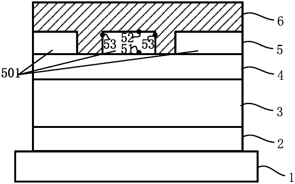
1. A display panel, comprising a first electrode, a light emitting structure, a second electrode and a scattering layer stacked in sequence; wherein,
the second electrode is a transparent electrode;
one side of the scattering layer away from the second electrode is configured as a light emergent side;
the scattering layer is of patterned array structures; and
the display panel further comprises:
a third electrode located at the one side of the scattering layer away from the second electrode.