| CPC H10K 50/121 (2023.02) [H10K 71/00 (2023.02); H10K 71/164 (2023.02); H10K 50/12 (2023.02); H10K 50/181 (2023.02); H10K 85/615 (2023.02); H10K 85/622 (2023.02)] | 9 Claims |
|
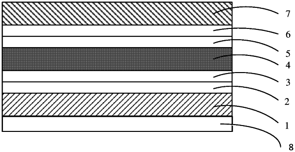
1. An OLED display device, comprising: a base substrate, and an anode, a hole transport layer, an electron blocking layer, a light-emitting layer, a hole blocking layer, an electron transport layer and a cathode which are sequentially arranged along a direction departing from the base substrate,
wherein a material of the light-emitting layer comprises a host light-emitting material and a carrier balance material doped in the host light-emitting material; and
the carrier balance material is used for balancing an electron mobility and a hole mobility of the light-emitting layer, and wherein
the host light-emitting material is a blue organic light-emitting material;
a doping concentration of the carrier balance material in the host light-emitting material is gradually changed in a thickness direction of the light-emitting layer; and
the carrier balance material comprises an electron blocking material.
|