| CPC H10B 63/22 (2023.02) [H10N 70/041 (2023.02); H10N 70/841 (2023.02); H10N 70/8833 (2023.02)] | 19 Claims |
|
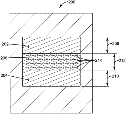
1. A selector device comprising:
a first electrode composed of a first metal having a first work function;
a second electrode composed of a second metal having a second work function;
a selector layer disposed between the first and second electrodes, the selector layer being composed of a dielectric material having a conduction band and a valence band defining a band gap of at least 5 electron volts and below 9.2 electron volts; and
dopant atoms disposed in the selector layer to form a sub-conduction band that is below the conduction band and above the first and second work functions;
wherein when a threshold voltage is applied across the first and second electrodes, and a magnitude of the threshold voltage exceeds an energy difference between the sub-conduction band and at least one of the work functions, but does not exceed an energy difference between the conduction band and the at least one of the work functions, an on-current will conduct through the selector layer.
|