| CPC H10B 43/27 (2023.02) [G11C 5/145 (2013.01); G11C 16/08 (2013.01); G11C 16/24 (2013.01); G11C 16/32 (2013.01); H10B 43/35 (2023.02); H10B 43/40 (2023.02)] | 17 Claims |
|
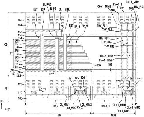
1. A semiconductor memory device comprising:
a cell array structure;
a peripheral logic structure comprising a first region comprising a first region of a substrate and a second region comprising a second region of the substrate, wherein the first region of the peripheral logic structure is disposed directly below the cell array structure;
first lower wirings disposed in the first region of the substrate;
second lower wirings disposed in the second region of the substrate;
a stacked structure, wherein the stacked structure is disposed on the first lower wirings, and the stacked structure comprises an interlayer insulating film and an electrode pad alternately stacked in a direction perpendicular to the substrate;
a vertical structure penetrating the stacked structure;
a tunnel insulating layer extending along sidewalls of the vertical structure;
a charge storage layer extending along sidewalls of the tunnel insulating layer;
a plurality of through vias disposed on the second lower wirings and disposed in the second region of peripheral logic structure, wherein the plurality of through vias are configured to electrically connect the second lower wirings and upper wirings, wherein the upper wirings are disposed in the second region of the peripheral logic structure;
a first amplification stage comprising the first lower wirings and configured to generate a first operating voltage to be applied to the electrode pad; and
a second amplification stage comprising the second lower wirings and the plurality of through vias, electrically connected to the first amplification stage, and configured to generate a second operating voltage to be applied to the electrode pad,
wherein the second region of the peripheral logic structure comprises a metal-insulator-metal (MIM) capacitor disposed above the plurality of through vias.
|