| CPC H10B 10/12 (2023.02) [H01L 23/528 (2013.01); H01L 27/0207 (2013.01); H01L 27/0924 (2013.01)] | 8 Claims |
|
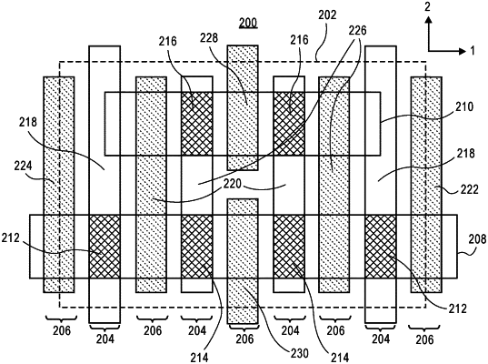
1. An integrated circuit structure, comprising:
a substrate;
a six transistor (6T) static random access memory (SRAM) bit cell on the substrate, the 6T SRAM bit cell comprising:
first and second active regions parallel along a first direction of the substrate; and
first, second, third and fourth gate lines over the first and second active regions, the first, second, third and fourth gate lines parallel along a second direction of the substrate, the second direction perpendicular to the first direction, wherein all of the first, second, third and fourth gate lines vertically overlap one of the first active region or the second active region, and wherein at least two of the first, second, third or fourth gate lines vertically overlap both of the first active region and the second active region.
|