| CPC H05K 5/0247 (2013.01) [H05K 5/0047 (2013.01); H05K 9/0033 (2013.01); H05K 9/0037 (2013.01)] | 6 Claims |
|
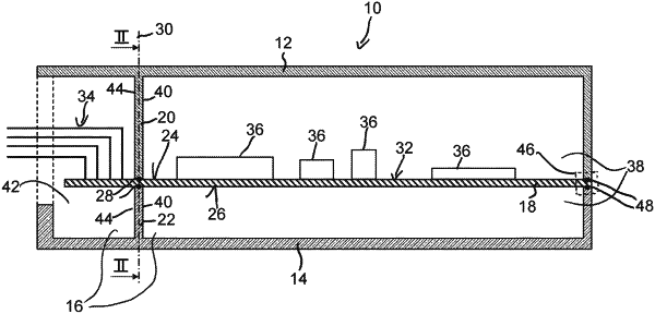
1. A device, comprising:
a housing with an electrically conductive housing top part and an electrically conductive housing bottom part, which together form an accommodation chamber of said housing;
a circuit board disposed in said accommodation chamber and having a top side and a bottom side, said bottom side is connected electrically to said top side via electrically conductive bores formed in said circuit board, wherein said circuit board further having electromechanical plug components which make possible an electrical connection to electrical components outside said housing, said circuit board additionally having electrical or electronic circuit components;
a first electrically conductive separating wall electrically connecting said electrically conductive housing top part to said top side of said circuit board; and
a second electrically conductive separating wall electrically connecting said electrically conductive housing bottom part to said bottom side of said circuit board, wherein said first electrically conductive separating wall and said second electrically conductive separating wall extend substantially in a common plane and subdivide said accommodation chamber of said housing into a first accommodation-chamber section on a first side of said first and second electrically conductive separating walls and into a second accommodation-chamber section on a second side, opposite said first side, of said first and second electrically conductive separating walls, and wherein said electrical or electronic circuit components are disposed on said circuit board such that said electrical or electronic circuit components are accommodated only in said first accommodation-chamber section, and said electromechanical plug components are disposed on said circuit board such that said electromechanical plug components are accommodated only in said second accommodation-chamber section;
an electrical connection formed by solder points between said first electrically conductive separating wall and said top side of said circuit board and/or an electrical connection formed by solder points between said second electrically conductive separating wall and said bottom side of said circuit board; and
said solder points being formed outside of, and spaced apart from, said electrically conductive bores formed in said circuit board.
|