| CPC H05K 1/0228 (2013.01) [H01L 23/49822 (2013.01); H05K 1/0298 (2013.01); H05K 1/111 (2013.01); H05K 1/115 (2013.01); H05K 1/181 (2013.01)] | 13 Claims |
|
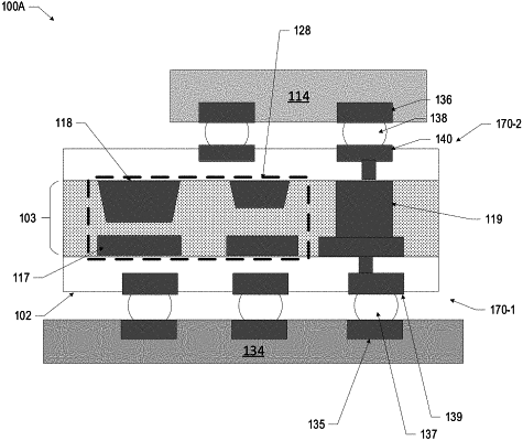
1. A microelectronic assembly, comprising:
a substrate layer having a surface, wherein the substrate layer includes a photo-imageable dielectric (PID) doped by an electroless catalyst, wherein the electroless catalyst includes one or more of palladium, gold, silver, ruthenium, cobalt, copper, nickel, titanium, aluminum, lead, silicon, and tantalum;
a first conductive trace having a first thickness in the PID, wherein the first thickness is between 4 um and 143 um; and
a second conductive trace having a second thickness in the PID, wherein the second thickness is between 2 um and 141 um, wherein the first thickness is greater than the second thickness, and wherein the first and second conductive traces have sloped sidewalls.
|