US 11,736,866 B2
Semiconductor structures
Rkia Achehboune, Edinburgh (GB); and Roberto Brioschi, Austin, TX (US)
Assigned to Cirrus Logic Inc., Austin, TX (US)
Filed by Cirrus Logic International Semiconductor Ltd., Edinburgh (GB)
Filed on Nov. 5, 2021, as Appl. No. 17/520,386.
Application 17/520,386 is a continuation of application No. 16/822,771, filed on Mar. 18, 2020, granted, now 11,223,907.
Claims priority of provisional application 62/822,268, filed on Mar. 22, 2019.
Claims priority of application No. 1905921 (GB), filed on Apr. 29, 2019; application No. 1905922 (GB), filed on Apr. 29, 2019; and application No. 1905923 (GB), filed on Apr. 29, 2019.
Prior Publication US 2022/0060835 A1, Feb. 24, 2022
Int. Cl. H04R 19/04 (2006.01); B81B 7/00 (2006.01)
CPC H04R 19/04 (2013.01) [B81B 7/0058 (2013.01); B81B 7/0061 (2013.01); B81B 7/0064 (2013.01); B81B 2201/0257 (2013.01); B81B 2203/0127 (2013.01); B81B 2203/0315 (2013.01); B81B 2207/012 (2013.01); H04R 2201/003 (2013.01)] 27 Claims
OG exemplary drawing
 
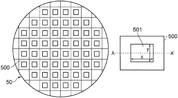
1. A semiconductor wafer comprising a plurality of primary die portions, each primary die portion configured to define a primary die following dicing of the semiconductor wafer, wherein at least one primary die portion comprises a plurality of apertures, each aperture extending through the semiconductor wafer from an upper surface of the semiconductor wafer to a lower surface of the semiconductor wafer, wherein each aperture is suitable for receiving a respective secondary die.