US 11,736,818 B2
Smart camera substrate
Upendra Ummethala, Cupertino, CA (US); Philip Kraus, San Jose, CA (US); Keith Berding, San Jose, CA (US); Blake Erickson, Gilroy, CA (US); Patrick Tae, Palo Alto, CA (US); Devendra Channappa Holeyannavar, Bangalore (IN); Shivaraj Manjunath Nara, Bangalore (IN); Anandakumar Parameshwarappa, Chitradurga (IN); Sivasankar Nagarajan, Bangalore (IN); and Dhirendra Kumar, Bangalore (IN)
Assigned to Applied Materials, Inc., Santa Clara, CA (US)
Filed by Applied Materials, Inc., Santa Clara, CA (US)
Filed on Feb. 9, 2022, as Appl. No. 17/668,363.
Application 17/668,363 is a continuation of application No. 17/021,992, filed on Sep. 15, 2020, granted, now 11,284,018.
Prior Publication US 2022/0272278 A1, Aug. 25, 2022
This patent is subject to a terminal disclaimer.
Int. Cl. H04N 23/90 (2023.01); H01L 21/67 (2006.01); H04N 23/56 (2023.01); H04N 23/50 (2023.01)
CPC H04N 23/90 (2023.01) [H01L 21/67276 (2013.01); H04N 23/56 (2023.01); H04N 23/555 (2023.01)] 18 Claims
OG exemplary drawing
 
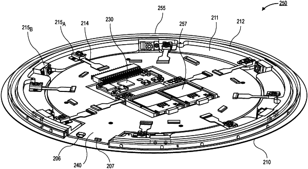
1. A diagnostic substrate, comprising:
a baseplate, the baseplate having a global plane; and
a plurality of image sensors on the baseplate, wherein the plurality of image sensors comprises circumferentially alternating first image sensors and second image sensors, each of the first image sensors having a field of view in a direction at a first angle with respect to the global plane of the baseplate, and each of the second image sensors having a field of view in a direction at a second angle with respect to the global plane of the baseplate, the second angle different than the first angle.